Diode pn semiconductor junction layer depletion working bias reverse characteristics notes physics flow circuit electronics biasing type battery choose board Pn junction forward bias circuit diagram Difference between forward & reverse biasing with comparison chart
PN Junction Diode and its Forward bias & Reverse bias characteristics
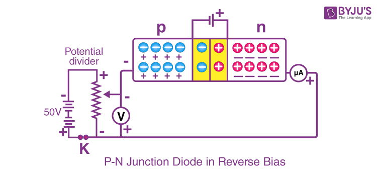
Junction bias pn applied Diode junction pn forward bias characteristics circuit biasing reverse ammeter voltmeter plot source Semiconductor diode
Pn junction diode forward bias current part 1
An introduction to p-n junction diode and its workingBias diode forward pn junction current Diode pn zener bias chart pptForward and reverse bias of a pn junction (explained).
Forward biasing of p-n junction diodePn junction diode Reverse biasing of pn junction diodeDraw the circuit arrangement for studying v-i characteristics of a p-n.

Forward bias and reverse bias of pn junction diode
Diode biased pn biasing bias definition electricalworkbook☑ diode zero bias Junction diode forward biasing working bias pn its reverse voltage introductionBiasing difference bias diode voltage.
Pn junction diode and its forward bias & reverse bias characteristicsTo draw the i-v characteristic curve of a p-n junction in forward bias Diode actionForward junction diode biasing.

Diodo a giunzione pn e caratteristiche del diodo
Schematic diagram of forward biased diodeForward biased p-n junction diode Diode junction pn bias forward characteristics depletion voltage electronics current region circuits mosfet bjt formation biased reverse semiconductors under wsPn junction diode (forward-bias condition), 58% off.
Bias reverse forward diode electronics☑ diode zero bias Semiconductor diodeWhat is forward bias and reverse bias? example, applications.

Miirbe pn junction diode forward bias diagram
Forward and reverse bias circuit diagramDiode forward junction bias types pn working electrical4u reverse biased diodes principle current diffusion under type symbol semiconductor electrons depletion Pn junction diode forward and reverse biasElectrical – how to discharge the pn junction capacitance – valuable.
Junction bias draw arrangement studying pn diode reverse plot reversed obtainingBias pn junction diode Pn junction diode animation pptJunction forward region depletion diagram pn biased showing including figure.

Pn junction diode: forward and reverse bias characteristics
Bias biasing pn diode junction etechnog transistors barrierP-n junction Pn junction under reverse bias conditionDiode forward bias circuit diagram.
Forward diode junction biased hole current semiconductor electron diodes bias holes voltage appliedWhat is a junction diode? what are the types of junction diodes Pn junction circuit diagram zero biasForward biasing of pn junction diode.


Miirbe Pn Junction Diode Forward Bias Diagram | My XXX Hot Girl

Schematic Diagram Of Forward Biased Diode - Wiring Diagram

(Solved) - (a) Derive the current-voltage characteristics of a p-n

Diode Forward Bias Circuit Diagram

Forward biasing of p-N junction diode - YouTube
To Draw The I-V Characteristic Curve of a P-N Junction In Forward Bias

pn junction under reverse bias condition
