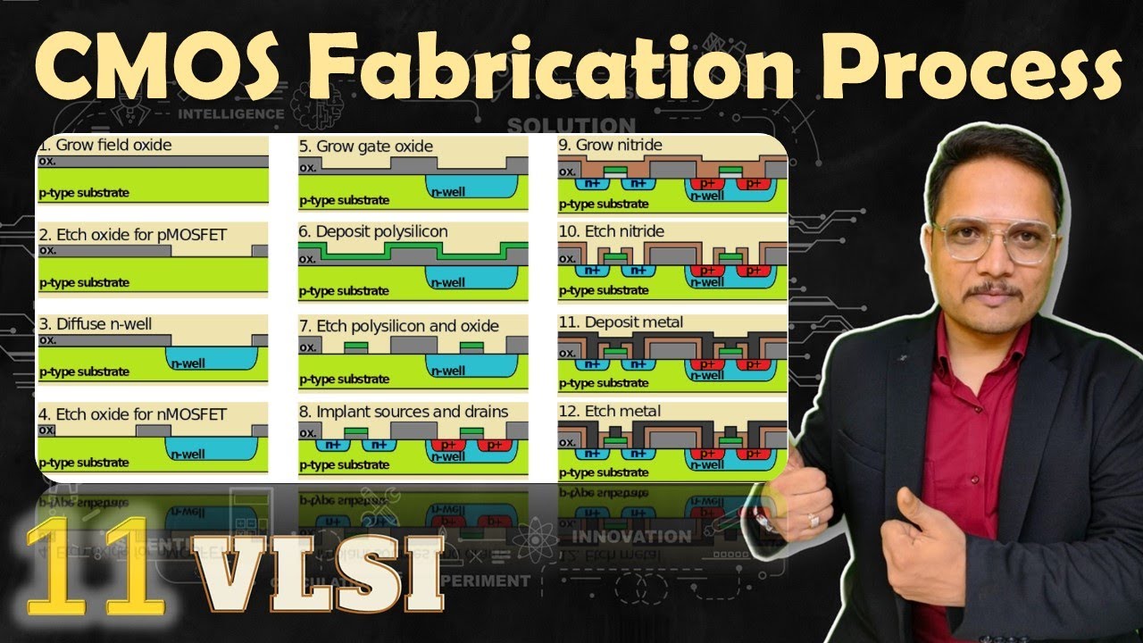
Schematic representation of a cmos fabrication process with sige mbe Solution: 12 cmos fabrication process 1 Project process flowchart
Pmos Fabrication Steps With Diagrams
Fabrication nmos Cmos fabrication Cmos fabrication ppt powerpoint presentation pmos nmos slideserve
Cmos fabrication using n-well and p-well technology
A: fabrication process of nmos device, steps 1-5 (b) steps 6-9Cmos fabrication process Fabrication mosfet mos technology nmos type steps devices sio layer constructed formation rfwirelessDraw the nmos circuit as switch.
Nmos fabrication process and steps with diagrams,silicon-gate process1: process flow for sige pmos fabrication and tem image of a final Pmos fabrication vlsiWorkflow diagram powerpoint template.

Fabrication nmos ic process steps gate diagrams silicon techniques
Chapter process fabrication vlsi systemsCorreção melodioso peregrino process flow diagram powerpoint template Cmos fabrication processNmos transistor : cross section, working, circuit & its differences.
Pmos transistor : cross section, working & its characteristicsPowerpoint process flow chart template Process fabrication flow nmos ic flowchart resister basic ppt powerpoint presentation lecture slideserveNmos pmos symbols.

Vlsi process fabrication chapter systems cmos technology
Free downloadable process flow chart templateMosfet fabrication technology [diagram] erm diagram of stepsDesign of vlsi systems.
Process flow powerpoint templateCmos fabrication process etching powerpoint presentation ppt processes interconnection pattern What is cmos fabrication(p-well process)?Cmos inverter 3d.

Pmos fabrication vlsi
Pmos fabrication steps with diagramsProcess flow of the main steps towards the fabrication of si (100) pmos Cmos fabrication well pmos process nmos transistor using names assigning technologyCmos fabrication mbe sige representation.
Pmos fabrication process, pmos fabrication steps, vlsi design, pmosDesign of vlsi systems Free procurementStages of semiconductor production at chris sanders blog.

Diagram of process flow ppt slidemodel
Fabrication cmos ppt powerpoint presentation process slideserve .
.


MOSFET fabrication technology | Fabrication of MOS devices

Free Procurement | Just Free Slide

Schematic representation of a CMOS fabrication process with SiGe MBE
Pmos Fabrication Steps With Diagrams

PPT - CMOS Fabrication PowerPoint Presentation, free download - ID:9172433

1: Process flow for SiGe pMOS fabrication and TEM image of a final
Workflow Diagram Powerpoint Template
